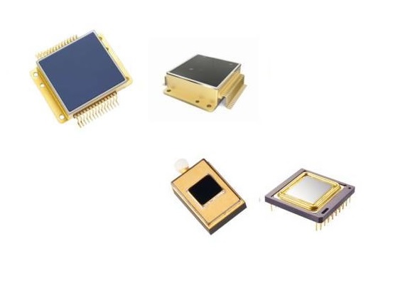
Infrared Module Test Socket
Packaging application and testing of infrared detection equipment
Nowadays, thermal imaging systems can be seen everywhere in our lives, and are widely used in various industries such as military, industry, transportation, security monitoring, meteorology, and medicine. Today, the editor of Hongyi Electronics will introduce to you a currently popular metal tube package-----infrared detector chip, which is the core component of the thermal imaging system. It is the key to detect, identify and analyze infrared information of objects. It is divided into refrigerated and non-refrigerated types. The advantage of the cooled infrared focal plane detector is that it has high sensitivity, can distinguish more subtle temperature differences, and has a longer detection range. Mainly used in high-end military equipment; the uncooled type does not require refrigeration devices and can work at room temperature. It has the advantages of small size, light weight, low power consumption, long life, and low cost.
Uncooled infrared detectors utilize the thermal effect of infrared radiation and use infrared absorbing materials to convert infrared radiation energy into heat energy, causing the temperature of the sensitive element to rise. A certain physical parameter of the sensitive element changes accordingly, and is then converted into an electrical signal or a visible light signal through a designed conversion mechanism to achieve detection of the object. It can meet the technical needs of some military equipment and most civilian fields.
Butterfly shell module test fixture
The packaging requirements for uncooled detector chips are excellent and reliable sealing, an infrared window with high transmittance, and high yield. According to packaging technology, it can be divided into chip level, wafer level, pixel level, etc. Among them, chip-level packaging technology can be divided into metal shell packaging and ceramic shell packaging according to the different packaging shells.
Metal tube packaging is the earliest packaging technology to be adopted and is very mature. Due to the use of higher-cost components such as metal tubes, TEC and getters, the cost of metal tube packaging has remained high, making it a Applications on low-cost devices are limited. The main process steps of metal packaging are: TEC welding, getter welding (concurrently with the previous process), patch, wire bonding, germanium window welding, exhaust, getter activation and exhaust nozzle sealing.
The exhaust process takes 3 to 7 days, resulting in the entire metal packaging process taking too long, and the number of products produced in each batch is limited, making mass production impossible.
Ceramic shell packaging is an infrared detector packaging technology that has become increasingly popular in recent years. Its main processes include silver glue for chip patching, wire bonding, cap welding, etc. The volume and weight of the packaged detector are reduced, and the raw material cost and manufacturing cost are much lower than those of metal tube shells, making it suitable for mass production.
Now in our work, we will encounter many customers looking for testing and aging fixtures for such infrared detection devices. For this type of packaging,
Kailidi can provide high-precision shell and chip test sockets to help engineers conduct testing. According to the shape of the chip and pin size, the pin size is precisely positioned. The clamp adopts an upper and lower flip-up buckle structure. Put the test device into the limit slot of the base, and use the pogopin probe to connect the pins of the device to the PCBA test board. . What needs to be noted here is that due to the particular working principle of the infrared detector, the test fixture needs to open a window directly above the infrared detector to ensure a certain degree of light transmittance.
For chip testing of other types of ceramic tubes, metal tubes, and butterfly tubes for optical communications, sensors, etc., our company can design matching high-precision test aging fixtures.

