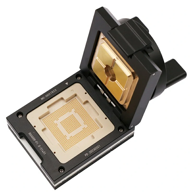


1. Actual requirements:
1.Package: BGA package WB-TePBGA II-689
2. Number of Pins: 689
3. Number of grounding connections: 0pin
4. Chip type: FPGA
5. Test requirements: chip function test
2. Demand analysis: BGA689-1.0-31*31 package chip is an integrated dual-core processor with a maximum clock frequency of 1067Mhz, L2 cache with ECC, and is equipped with SRAM memory function. The DDR part supports 800MT/s. , up to 32G memory. There are no special high-speed requirements for other interfaces. The USB function only has the performance of USB2.0, so it requires up to 1067Mhz. A separate probe needs to meet this requirement. In addition, the dual-core chip has high power consumption and needs to be configured accordingly. heat sink to assist in heat dissipation during operation;
3. Production: BGA689-1.0-31*31 is a standard plastic ball array chip, referred to as WB-TePBGA. Its dimensional tolerance needs to refer to ASME Y14.5M-1994. It should be noted that the package has plastic bulges. part, so the heat dissipation part needs to be kept away from the air, so as to facilitate the fit between the chip and the heat dissipation structure and reduce the thermal resistance, which is beneficial to the heat dissipation performance during testing. Another issue is the matching of probes and low impedance. If this is done well, the chip will generate less heat, and the performance test results will be better.
4. During the production process, each component is strictly tested to ensure that the components fit well in the large array chip test socket. The probe performance can only be assembled after confirming its performance parameter data. After the test socket is produced, it can be sent to the user for final testing and verification.

