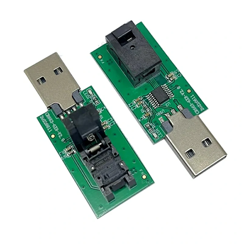


1. Product introduction:
1.Package: LGA8 QFN8 DFN8 package
2. Number of Pins: 8
3. Number of grounding connections: 0pin
4. Chip type: SD NAND SPI NAND, chip manufacturers include: Brontosaurus, MicroFont, CS Creation, etc. Supports 6*8mm package (off-the-shelf); 9*12.5mm size needs to be customized
5. Test requirements: chip speed test, aging test and programming use
2. Demand analysis: Users generally need to do IQC on the chip, that is, receiving quality inspection, and functional aging test during shipment. This requires the test socket to meet the test of industrial-grade aging environment (-40~85℃). It also needs to meet the requirements of the SDIO protocol and SPI transmission rate.
3. Production: The product needs to meet the above chip testing and burning requirements. In addition to a test socket, the corresponding main control GL823K also needs to be used to transfer the SD protocol to USB to facilitate user use and testing. For burning, you need to cooperate with the burning software provided by major chip manufacturers.
4. After production is completed, all dimensions of the test socket will be inspected for quality, and each dimension marked on the drawing will be strictly inspected. Once confirmed, it can be assembled; while assembling, 10pcs samples need to be repeatedly manually adapted and verified; assembled at the same time After completion, the same inspection is required. Once all inspection passes are passed, the products can be shipped into the warehouse.

