
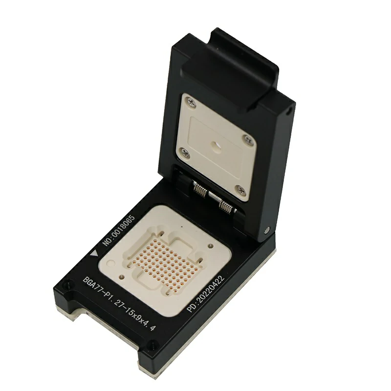
BGA77 DC/DC high current test socket
1. Actual requirements:
1.Package: BGA package
2.Pin number:77pin
3. Spacing: 1.27mm
4. Chip type: DC/DC chip test socket
5. Testing requirements: chip functional debugging, programming and mass production
2. Demand analysis: BGA77 is a relatively special power chip recently. Its function is DC/DC power supply function, with a total of 4 channels of output. The continuous current output of each channel is DC 4A, and the output peak value is 5A. When its function is DC to DC, it converts the voltage from 4V to 14V into a voltage of 0.6V~5.5V, releasing higher current and heat, and its power consumption is as high as 5.5W. Its chip size is 9*15*5.01mm and the pitch is 1.27mm. .
3. Based on the performance requirements of the above chip, you also need to understand the location of the chip's multi-channel pin map and confirm the number and distribution of its input and output pins. The BGA77 chip test socket needs to match the multi-channel high current chip during use. It is necessary to know the pin assignment of each channel, so as to assist in completing the corresponding test socket design;
Since this chip is mainly for power supply testing and is related to power conversion, through the evaluation of multiple channel test currents and the corresponding current of high-current probes, it can basically respond to the demand at a slow speed. Vin is generally 2pin and Vout is 3pin. Using Only high current probes can match such a large current.
In the process of power conversion, the problem of chip heat dissipation needs to be addressed. The power consumption of the chip is 5.5W. The top of the test socket needs to be used for heat dissipation. The metal shell is used to conduct the heat to the shell and assist the chip to dissipate the corresponding heat.
The spacing between chips is large, which facilitates the design and processing of the pin plate and external structure of the test socket. Due to the size of the chip, the pressure of the test socket needs to be sufficient and the buckling force must be ok to avoid poor contact;
4. During the production process, each customized component is strictly inspected to confirm that the structure of the chip is within the allowable range. Only after all components are confirmed to be ok can they be assembled, and the overall inspection is completed before shipment.


